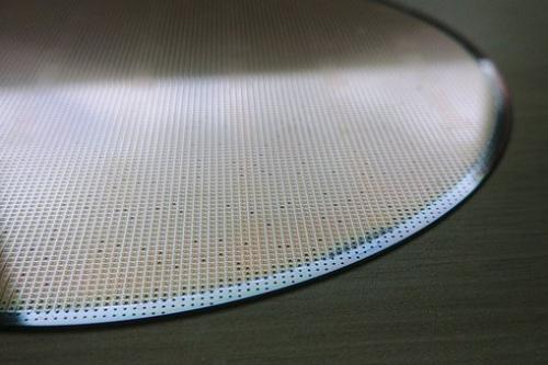
it is reported that ferrotec announced an investment of about 500 million yuan to enter the precise regeneration business of 300 mm semiconductor wafer in china.
ferrotec (china) was founded in 1992 in hangzhou, zhejiang province. it is a diversified enterprise set up in china by ferrotec co., ltd. of japan, which integrates product r & d, manufacturing and sales. more than 20 companies under its management are located all over china, providing customers at home and abroad with advanced materials, devices, equipment and system solutions. ferrotec co., ltd. has a global marketing network. it has established a base company in china, japan, the united states, germany, france, italy, spain, russia, south korea, malaysia and other places. it is a multinational group with a number of high-end production technologies.

in august last year,ferrotec (anhui) changjiang semiconductor material co., ltd., a comprehensive high-tech enterprise engaged in electronic technology and material science research services jointly established by hangzhou dahe thermo-magnetics co.,ltd., shanghai shenhe thermo-magnetics electronics co.,ltd., and tongling development investment group co., ltd., was officially established with a total investment of 1 billion yuan, covering an area of 75 mu, and a new factory building of 5.56 10000 square meters, including 37600 square meters of production workshops and 18000 square meters of auxiliary rooms.
the construction period of the project is planned to be 15 months. after the completion of the project, an annual production line of 1.8 million 300 mm semiconductor wafer precise regeneration will be formed. it is another important strategic decision of ferrotec (china) in domestic layout, which fills in the gap of domestic large-scale semiconductor wafer precision regeneration business. on march 18 this year, the roof of the complex building of the project was sealed, and the preliminary planning and construction approval of the project had been completed successfully.
after the establishment of the company,hangzhou dahe thermo-magnetics co.,ltd.carried out an internal review on the wafer recycling business. with the growth of china's 300 mm wafer market, the demand for recycled wafers is expanding, while the number of global 300 mm wafer recycling plants is limited, and they are concentrated in the united states, japan, taiwan and other places. at present, the semiconductor wafer polishing technology and precision parts recycling and cleaning technology developed byhangzhou dahe thermo-magnetics co.,ltd.can be transferred to the wafer recycling business. in view of the above reasons,hangzhou dahe thermo-magnetics co.,ltd.decided to invest in the business.
in china, in addition to yangtze river storage, which has begun to use 300 mm wafers to produce nand, dram has also announced the entry of several companies. foreign enterprises such as samsung, sk hynix and other memory manufacturers will focus on capacity expansion, and the demand for 300 mm wafers is expected to increase.